The Fabrication Process of Flex PCBs
Fabrication Process of Flex PCBs
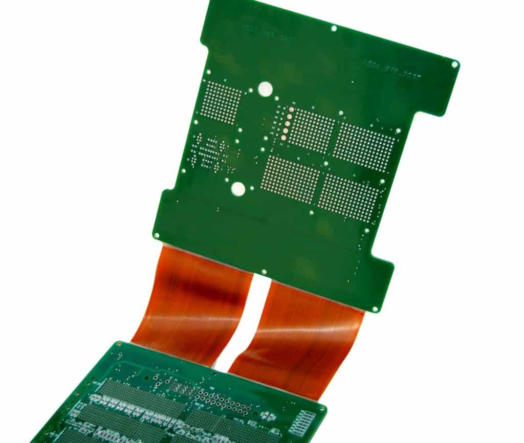
Unlike rigid PCBs, which are rigid in shape and form, flex pcb fabrication can be bent or folded. This makes them ideal for use in tight spaces such as handheld devices. However, a flexible circuit board also needs to be able to withstand repeated bendings without being damaged. This is why flex PCB manufacturing requires special techniques and processes to ensure a high quality product.
The fabrication process of a flex PCB begins with design, where the layout is carefully planned using software. This is crucial for the success of the final product and helps to minimize cost by ensuring that every element is used effectively. Once the layout is approved, the manufacturing process can begin. Rigid flex manufacturers start by fabricating the rigid sections of the board, which are made from materials such as FR4. Once these are completed they apply copper cladding to the substrate, forming the conductive traces and pads.
Flex PCBs, or flexible printed circuit boards, are essential components in modern electronics, enabling flexible and lightweight designs for a variety of applications. The fabrication process of flex PCBs involves several intricate steps to ensure reliability and functionality.
Once the copper layer has been etched, it is covered with an adhesive-free or adhesive-based coverlay, which protects the surface of the flex section from scratches and UV radiation. This is typically an additional polyimide film, though some manufacturers also use photoimageable solder mask. This is then cured on the top and bottom of the flex sections.
The Fabrication Process of Flex PCBs
The next step is drilling, where the positioning holes are drilled mechanically. The drilled holes are used for mounting components on the PCB. The positioning holes must be positioned with care as they will need to withstand repeated bending and twisting, as well as being subjected to environmental tests such as humidity, temperature cycling and shock.
Next, the flex and rigid sections of the board are laminated together with the outer final copper foil layers. This process is referred to as lamination, and can be performed either manually or with automated machines. The final step is etching the circuit pattern, and this is usually done by dipping the laminate in an etchant solution or spraying it with acid. Once the etching is complete, the final outer layer copper patterns are drilled with holes for pad and blind vias if needed.
The process typically begins with the design phase, where engineers create a layout considering the flexible nature of the board and the specific requirements of the application. Once the design is finalized, it undergoes a series of steps:
The flex sections are then die cut from the production panel using high-precision male and female punches or chemically milled dies, depending on the final product requirements. The flex PCBs are then inspected for errors using optical inspection, and if necessary, electrical tests are conducted. Once the flex PCB has passed inspection, it is sent for final quality control. Afterwards, it can be cut to size, packaged and shipped for distribution.